
Samsung Galaxy A03 Core (SM-A032F / SM-A032M) ISP Pinout & Dump File
Samsung Galaxy A03 Core (SM-A032F / SM-A032M) ISP Pinout & Dead Boot Repair Dump File
Before proceeding with chip-level hardware repair on the Samsung Galaxy A03 Core (SM-A032F / SM-A032M), it is crucial to understand the eMMC pinout mapping. The Samsung A03 Core ISP (In-System Programming) pinout allows technicians to directly read, write, and repair the eMMC 5.1 BGA memory without desoldering the chip from the PCB. You can use this with EasyJTAG Plus, UFI Box, Medusa Pro II, MIPI Tester, and UMT ISP Tool for dead boot recovery, unbricking, and partition restoration.
Samsung Galaxy A03 Core ISP Pinout Diagram (High Resolution):
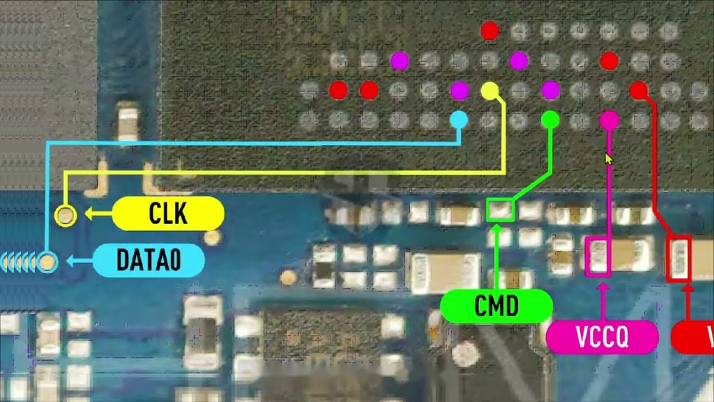
[ Click Here to Download / View Full Resolution Original ISP Pinout Diagram ]
📌 Jumper Connection Points & Color Guide:
- CLK (Yellow Line / Pad): Clock signal line. In case of CMD/CLK timeout in EasyJTAG or UFI, add a 100-ohm resistor inline.
- DATA0 (Cyan Blue Line / Pad): 1-Bit Data 0 transfer line for high-speed eMMC communication.
- CMD (Green Line / Pad): Command signal connection to initiate eMMC handshake.
- VCCQ (Magenta / Pink Box 1.8V): Connect to the 1.8V logic power capacitor.
- VCC (Red Box 3.3V): Connect to 3.3V core power (or plug in standard USB Type-C cable for VCC power supply).
- GND (Ground): Solder directly to the motherboard ground shield.
🛠️ Step-by-Step Dead Boot Repair & Dump Flashing Guide:
- Preparation: Disassemble the Samsung A03 Core and safely remove the motherboard from the casing.
- Shield Removal: Carefully remove the metal shielding covering the eMMC chip using a hot air rework station (or shield cutter) to expose the jumper test points.
- ISP Soldering: Solder thin jumper wires (0.02mm or 0.1mm) to CLK, CMD, DATA0, GND, VCC (3.3V), and VCCQ (1.8V) as shown in the microscope diagram.
- Hardware Connection: Connect the ISP adapter to your EasyJTAG Plus / UFI Box socket.
- Software Configuration: Launch the eMMC Tool suite, select 1-Bit Bus Width, and set Voltage to 1.8V (VCCQ) / 3.3V (VCC).
- Identify & Backup: Click Identify eMMC / Check. Always make a full backup of security partitions (EFS, NVRAM, PERSIST) before writing the dump.
- Write Dump File: Flash ROM1 (Userarea), ROM2 (Boot 1), ROM3 (Boot 2), and configure the ext_csd partition.
- Final Flash: After writing the dump, disconnect the ISP wires, assemble the motherboard, and flash the official stock 4-file firmware via Odin Flash Tool to complete the repair.
⚠️ Important Technician Notes:
- Always verify microscope solder joints under proper magnification to prevent accidental bridging.
- Use proper ESD (Electrostatic Discharge) protection while working on the mainboard.
- Keep jumper wire length as short as possible (under 5–7 cm) for stable high-speed clock communication.
Supported Box
- Mipi Tester
- Easy J-Tag
- F64
- Medusa
- All Boxess
ISP Pinout and Dump
Supported Box
- Any ISP Adapter
- UFI
- Easy-J-Tag
- Mipi Tester
- Medusa